|
introduction
PIN photodiodes are cheap semiconductor devices, commonly used in optoelectronics for detection of light, usually in visible or infrared range. Analysing their internal structure and technical parameters one may find some similarities to semiconductor radiation detectors used in high-resolution spectrometry. This allow us to expect that a low-cost PIN photodiodes could be used to direct detection of X/gamma radiation in a range up to about 100 keV.
There are only few papers that report the application of PIN photodiodes for direct detection of radiation, but always using a very expensive low-noise charge preamplifier. We have not only checked that a cheap PIN photodiodes can be applied to this aim but also decided to design a dedicated charge-sensitive preamplifier based on widespread discrete components only. With less than 20 Euros we have built a complete X/gamma-ray spectrometer. Energy resolution (FWHM) of 1,5 keV was achieved for 59,5 keV line taken with Am-241 radioactive source.
PIN photodiodes
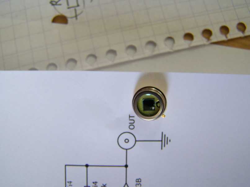
A typical PIN photodiode is shown in Fig.1.
![[img]](dioda_w_svg.jpg)
Fig.1 Cross-section of PIN photodiode
It consists of the highly-doped transparent p-type contact layer on the top and the n-type layer on the bottom. The most important for our application is the thick intrinsic (undoped) layer between the n and p layers.
The above structure is necessary for one basic requirement. Photons should be absorbed in the depletion region of the photodiode to ensure that the generated electrons and holes are separated by an electric field and contribute to a photocurrent, keeping the transit time as short as possible.
This implies that a depletion region width larger than the absorption length should exist in the detector. This is easily assured by making the absorbing layer undoped, because only a very small voltage is required to deplete the undoped region. The additional advantage is that the recombination/generation time constant is longer for undoped material, providing a minimal thermal generation current (leakage current).
The most important in a spectrometric application are noise characteristics of the photodiode. Two parameters have majorl contribution to noise level: leakage current and capacitance of the photodiode. Existence of the intrinsic layer lowers both the leakage current and the capacitance of junction so it is possible to achieve good energetic resolution even at room temperature.
The upper limit of photon's energy, which can be registered by detector, is determined by thickness of depletion layer. The total energy of photon should be absorbed there to properly measure its energy so the thickness of the layer should be larger then absorption length of a particle. When one calculates it for typical thickness of intrinsic layer, which is about 80 mm, he will see that photons with energy up to 100keV can be registered. Of course an exponential decrease of efficiency as a function of photons' energy will also be observed. The larger active area of a photodiode means better efficiency but it also increases leakage current which has significant influence on energy resolution of the detector. Since the photodiodes we used were designed to detect visible light during the operation they have to be kept in a tight metal box. A plastic cover of the photodiode was mechanically removed do avoid additional scattering and absorption of photons.
principle of operation
In the energy region of our interest there are two main processes of photon's interaction with solid matter: photoelectric absorption and Campton scattering. One should have in mind that photon do not ionize matter directly. Both of mentioned processes transfers photon's energy to electrons which then ionise matter directly.
When light strikes a photodiode, the electron within the crystal structure of silicon becomes stimulated. The energy which is required to generate one electron-hole pair in silicon is 3,6 eV. In average if the energy quanta is greater than 3,6 eV the electrons are pulled up into the conduction band, leaving holes in the valence band. These electron-hole pairs are generated throughout the P-layer, depletion layer and N-layer materials. In the depletion layer the electric field accelerates the electrons towards the N-layer and the holes towards the P-layer. In this way the electron-hole pairs which are generated in proportion to the amount of incident light are collected on the electrodes of the N- and P-layers.
When one wants to calculate a number of generated charges he should divide the deposited energy by 3.6 eV. This means that for X-ray photon generates only few thousands of electrons and since there is no internal gain in a photodiode, a very sensitive read-out electronics is a must.
front-end electronics
As it was mentioned above only few thousands electrons are generated by an X-ray photon. If one wants to achieve high energy resolution, for example with FWHM equal to 2 keV for 59,5 keV 241Am line, this implies that equivalent noise charge should be smaller then 200 electrons. At room temperature and using only discrete components this is a real design challenge. Electronics can be divided into two main parts: the preamplifier circuit and the shaper. General scheme is presented in Fig.2.
![[img]](detektor_web.jpg)
Fig.2 General scheme of preamplifier and shaper. Respectively on left and right.
preamplifier
Special attention must be paid to the first stage which is the most critical. The integrating circuit has been used, which transforms current pulse into a voltage pulse with an amplitude proportional to a charge carried by the current pulse. After many considerations and attempts we have decided to use the OPA657 operational amplifier. Thanks to the JFET input transistor it has very good noise characteristics. The applied circuit should also have high gain and be linear.
Because the pulse amplitude at the amplifier output is inversely proportional to capacitance of the feedback loop, this capacitor should be possibly small. To avoid saturation of the preamplifier it is necessary to discharge the capacitor which is done by a resistor connected in parallel to the capacitor. It should be pointed out that this resistor is an additional source of noise so its resistance should be possibly high.
shaper
The amplitude of a voltage signal in the output of preamplifier is only about few mV so additional amplification and noise-filtering is a must. This is done by a circuit called "shaper". Every signal has its natural spectrum in a frequency domain and a noise spectrum is added to it. When one uses filters it is possible to improve the signal to noise level. We have decided to use one differentiator and three integrators - (CR)-(RC)3 filter - with equal shaping time constants for each stage. To achieve the optimum noise performance of the system we have investigated experimentally shaping time constant dependence. Details can be found in the results section.
During design and assembly many technical problems have also been overcame. Because the first stage of circuit has very high gain it is very sensitive to any external disturbance, especially electromagnetic waves in a wide range of frequencies from power lines. Due to this a lot of efforts were done to ensure proper shielding.
results
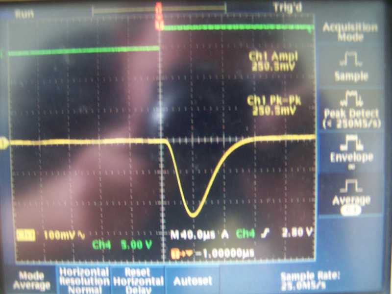
In the first tests of detector system a voltage pulse from generator was injected at the preamplifier input. To achieve the optimum noise performance we have begun with tests of many available in shops PIN photodiodes to find the ones which would be most interesting in our investigations. It was found that the PIN photodiode SFH206K from Osram shows the best noise performance. After this, we have investigated the bias voltage of a photodiode and shaping time constant dependence on equivalent noise charge which is shown in Fig.3. The optimal peaking time constant occurs at 10 us and the ENC was found to be 190 electrons.
![[img]](enc_vs_shapetime.jpg)
Fig.3 ENC of the detector vs. shaping time
The response of photodiode for detection and spectrometry of low-energy gamma and X-rays was studied through the use of a 241Am and 238 Pu radioactive sources. The line from Cu fluorescence radiation, which was used for calibration, is also seen on the spectra thanks to special geometry of the measurements. Results are shown in Fig.5 and Fig.6. It should be pointed out that lower energy lines are detected with higher efficiency which can be easily understood. Calculating area of the peaks it is possible to find the dependence between energy of quanta and the efficiency of detection. Results agree with theoretical predictions.
![[img]](cal.jpg)
Fig.4 Spectrometer calibration curve
The channel numbers of the fitted peak centroids were plotted versus photons energies from 10 up to 60 keV to verify linearity of a detector system and the results are presented in Fig.5. Hereby, an excellent degree of linearity over the full energy range is observed.
![[img]](am.jpg)
Fig.5Energy spectrum of 241Am
![[img]](pu.jpg)
Fig.6 Energy spectrum of 238Pu
conclusions
It has been shown that a low-cost commercial PIN photodiodes are appropriate for detection and spectrometry of X-ray and gamma radiation even when they are coupled to an inexpensive "home-made" preamplifier. With less then 20 Euros it was possible to built a complete spectrometer. The achieved resolution (FWHM) which is about 1.5keV is sufficient for many applications and there are still many possibilities for improvements. Beside low-cost detectors based on commercial PIN photodiodes have many advantages. They can operate at room temperature, do not require high voltage power supply and have small size. This indicates many possible applications which may include measurements of radiation inside phantoms, application to X-ray Fluorescence Analysis or in students' laboratories.
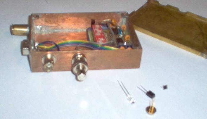
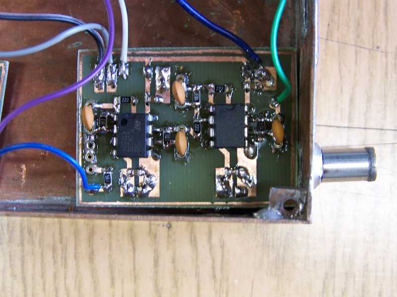
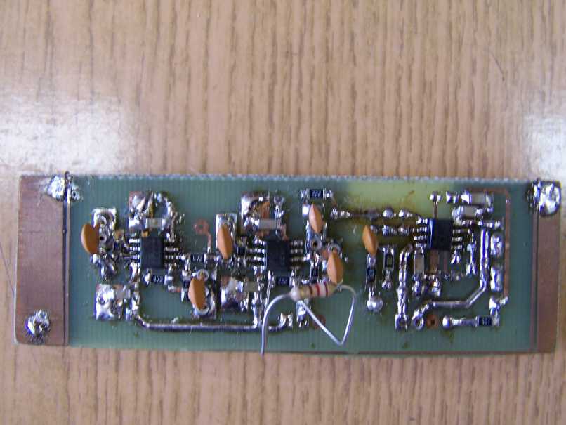
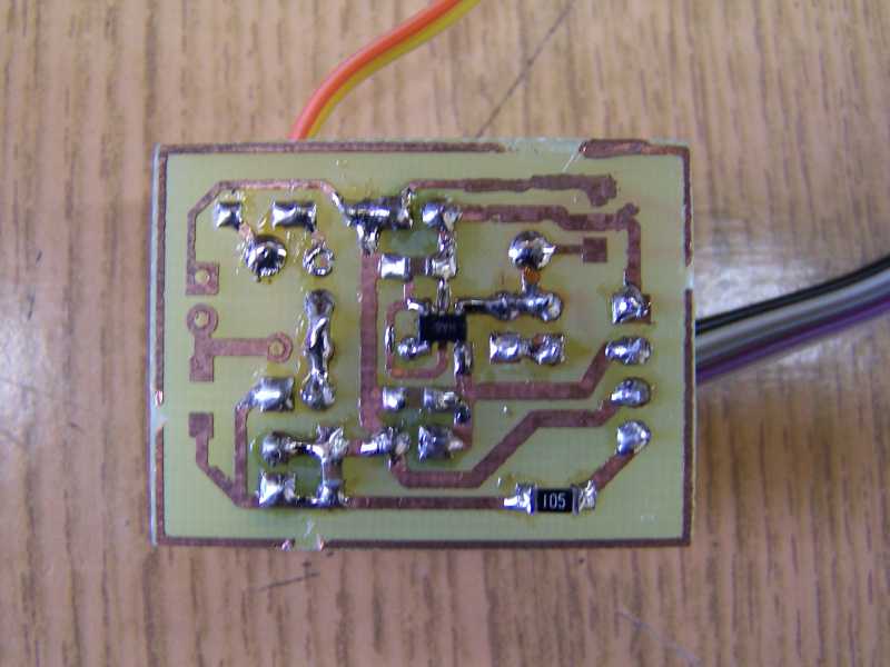
photos
authors
Authors of the project are Bartłomiej Szpak and Szymon Kulis.
|